MAX 10 POLLEN BOARD
This project was my Junior Design group’s final project for ECE 342: Junior Design II at Oregon State University.
The Max 10 Pollen Board is a FPGA development board designed for digital signal processing that was initially
intended to contribute to the Music Box project that my Junior Design group was assigned.
![]()
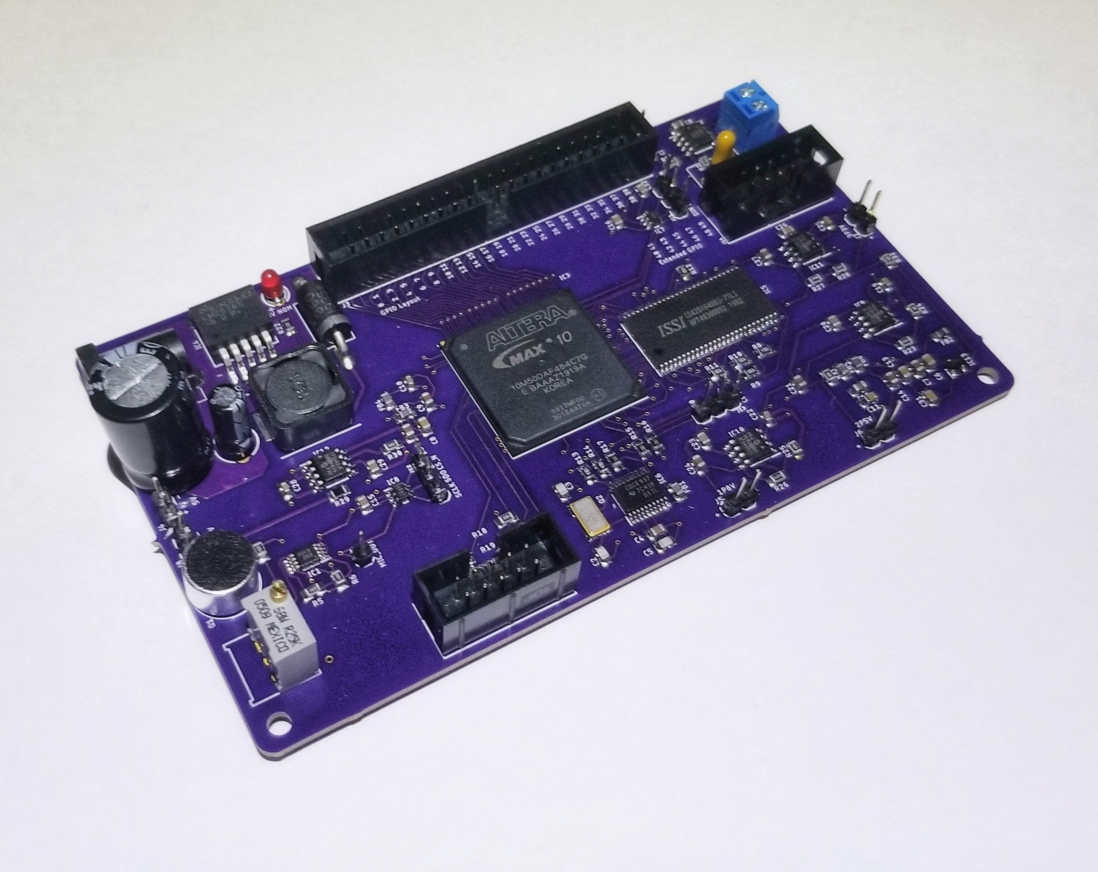
My responsibility for the Music Box project was to make the main PCB that would operate as the central processor. Our group elected to center the project around an FPGA. This component was selected for the value as an educational exercise in working with a potentially very power component. FPGAs are becoming increasingly popular in the hobbyist and professional community as a way for simulating computer architectures, creating fast parallel task performance and allowing hardware to be adapted once at the customer. Our group saw that value of this component and acknowledged that we had gaps in our knowledge about their operation and wished to know more. In retrospect, this project would have been much more successful in the task of creating of a Music Box if we had centered the design around a microcontroller that had a familiar architecture (AVR comes to mind). However, that’s not what being a student is about and that’s not what innovation is about.
I have learned so much more about PCB design from doing the research for this project. The primary challenge was
centered around the Altera MAX 10 FPGA that was selected as the central processor due to a donation from Intel to
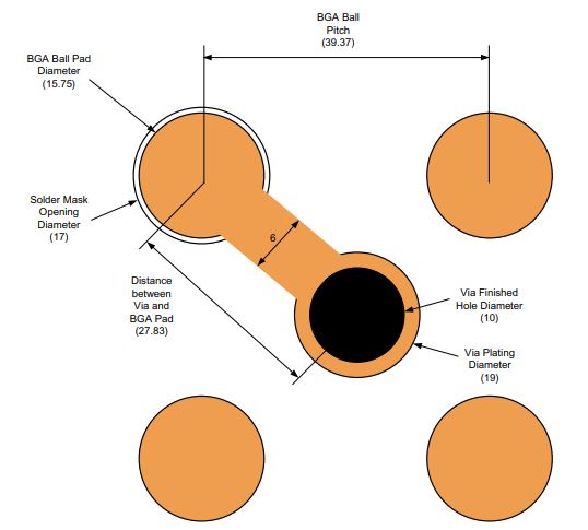
Oregon State University. The package type of the FPGA was a FBGA-484 package. A 484-Ball Grid Array that had a Ball
Pitch of 39.37mils (One thousandths of and inch) which left enough room to fit a via that could be no larger than
10mil (The absolute minimum size of via allowed by OSHPark; who manufactured the PCB). Since we knew that it was
possible to layout the package given the requirements from OSHPark and the package itself we still had the problem
a physically soldering the package once you have the PCB and the package. The secret to cracking that was in circuit
board surface finishes!
After doing research (and messing around with the settings on PCBWay’s quote calculator) I found that there are multiple surface finishes that you can get for the top layer of copper on your circuit board. The standard that is selected by default is HASL (Hot Air Solder Leveling), which is simply another layer of solder that is usually wave soldered on the copper of the blank PCB. The problem is that HASL is NOT completely flat! The wave soldering generates a surface that has collections of gunked solder that sticks together. These gunks are usually removed with hot air knives that go over the board, but still not flat enough to layout a package like the FBGA-484 without some balls of the package being lifted off the contacts. I looked for alternatives to the HASL surface finish I’ll list all that I found for completeness.
HASL (Hot Air Solder Leveling)
The standard, typically SnPb (Tin Lead) based, finish that leaves a surface too uneven for large BGA packages. Also available in lead-free variants.
ENIG (Electroless Nickel Immersion Gold)
Electroless nickel plating covered with a thin layer of immersion gold, which protects the nickel from oxidation. It is possible for a ‘black-pad’ nickel phosphorus to form during the electroless nickel plating step, more specifically due to the solder mask sulfur substances leaching into the plating bath. This creates an excellent flat surface that is perfect for large BGA packages. This ultimately is what my Design Group went with.
OSP (Organic Solderability Preservatives)
This finish is a safer step above lead-free finishes. It is a water-based organic compound that selectively bonds to copper and protects the copper until soldering. So cool! However, you usually only see this finish if it is legal requirement from a government.
Hard Gold
 Everything is solid gold. Extremely durable and recommended for uses in high contact areas. Think areas like the on a multimeter rotary, where the
contacts are brushing against it for its entire lifetime.
Everything is solid gold. Extremely durable and recommended for uses in high contact areas. Think areas like the on a multimeter rotary, where the
contacts are brushing against it for its entire lifetime.
IAg (Immersion Silver)
Comparable in surface level to HASL but with the chemical advantages of silver (best conductor). Also, chemical disadvantages of silver, surface quickly oxidizes.
ENEPIG (Electroless Nickel Electroless Palladium Immersion Gold)
Think ENIG++. This surface finish adds the Palladium Immersion which prevents the ‘black pad’ effect that is a great drawback to the ENIG surface finish. Also retains the near perfect flat finish of ENIG. My Design Group did not go with this finish due to cost and unavailability.
Plain Copper
Not used for industry applications anymore. Tarnishes too quickly. Popular among DIYers for chemical etching with copper clad plates and ferric chloride (I would love to try this someday :^))
We went with ENIG finish and the why and some of the how of this part of the project was worked out. Layout of the circuit board was completed in Autodesk EAGLE CAD as a 4-layer board layered (from top to bottom) Signals/Power/GND/Signals. The circuit board was sent to OSHPark for it to be manufactured.
 For populating the circuit board, Matthew Shuman (an instructor at Oregon State University) instructed our group to expand our experience by reaching
out to Hi-Tek Electronics in Salem, Oregon to get our board professionally populated. This was elected to be an excellent choice since it would offer
a chance to work with industry professionals (an experience that very few students get) and certainty that the BGA package was laid out correctly.
For populating the circuit board, Matthew Shuman (an instructor at Oregon State University) instructed our group to expand our experience by reaching
out to Hi-Tek Electronics in Salem, Oregon to get our board professionally populated. This was elected to be an excellent choice since it would offer
a chance to work with industry professionals (an experience that very few students get) and certainty that the BGA package was laid out correctly.
 Interfacing with Hi-Tek was very simple, I sent them a BOM, Gerber files, centroid file (describes the physical location of parts on the board), the
components we had on-hand and Hi-Tek handled the rest. Thanks to efforts from Matthew Shuman and the general manager at Hi-Tek, Darryl Gordon. My Design Group got
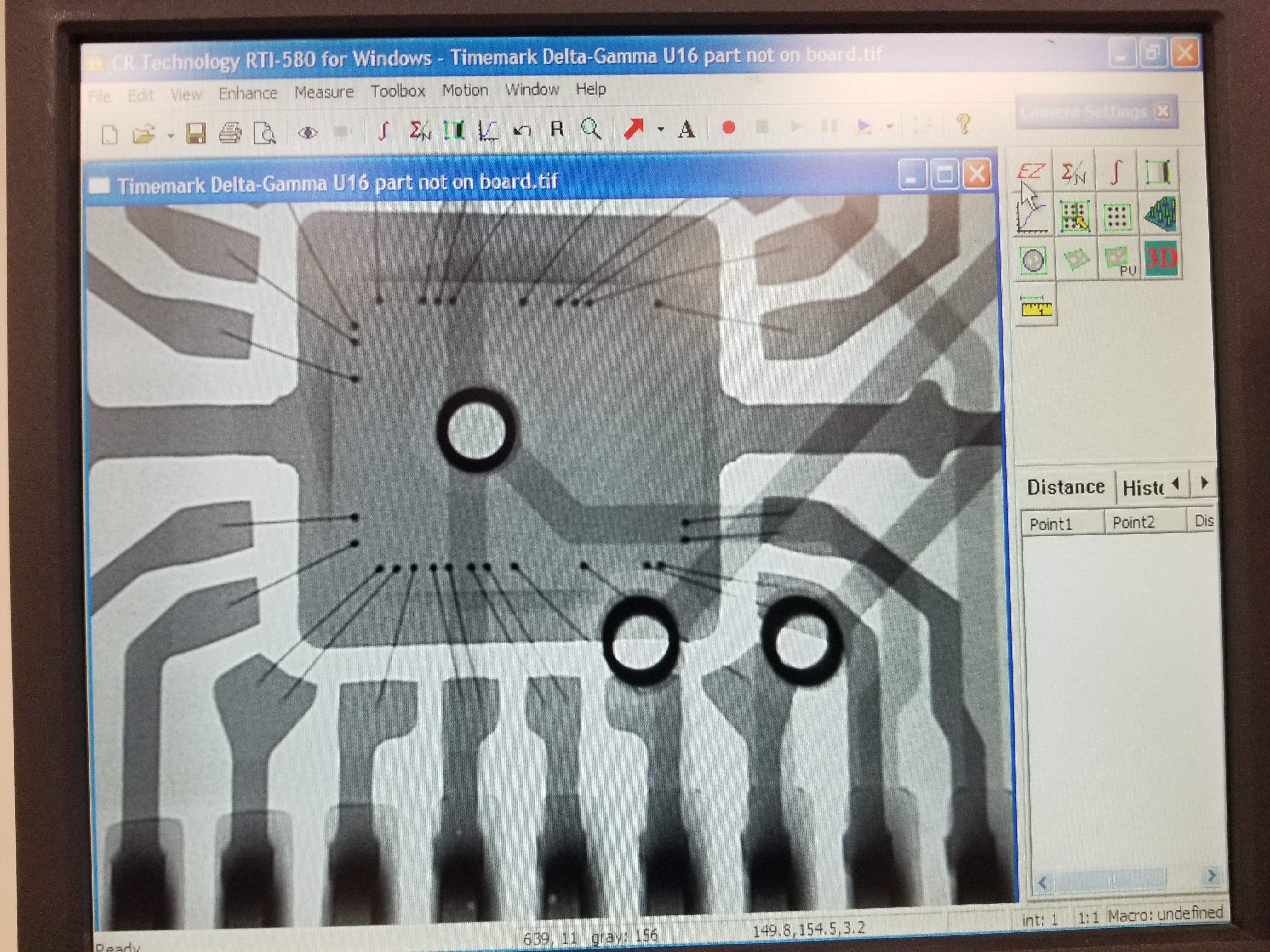
the opportunity to see the x-rays and process they go though when populating a board. I asked how I could have improved my board to make their job
easier. The answer was simply: fiducial markers. It is standard to include markers on three of the four corners of your board so a person and machine
can quickly determine the orientation of the board. Would never have know otherwise, this was an extremely valuable experience.
Interfacing with Hi-Tek was very simple, I sent them a BOM, Gerber files, centroid file (describes the physical location of parts on the board), the
components we had on-hand and Hi-Tek handled the rest. Thanks to efforts from Matthew Shuman and the general manager at Hi-Tek, Darryl Gordon. My Design Group got
the opportunity to see the x-rays and process they go though when populating a board. I asked how I could have improved my board to make their job
easier. The answer was simply: fiducial markers. It is standard to include markers on three of the four corners of your board so a person and machine
can quickly determine the orientation of the board. Would never have know otherwise, this was an extremely valuable experience.
 There was a lot of excitement when we first got out PCBs back from Hi-Tek and it was time for testing. Plugging the PCB in to the 9V jack I was kicking
myself seeing every design flaw. Wishing I had added 0 Ohm resistors to disconnect assemblies so they could be tested individually, seeing that there
wasn’t enough clearance for the upper right screw to fit with the terminal block connector in-place, wishing I made a 3mm hole that connected to ground
rather than a straight drill, get rid of the debug header on the clock nodes for fear of it interrupting the signal. I can go on forever.
There was a lot of excitement when we first got out PCBs back from Hi-Tek and it was time for testing. Plugging the PCB in to the 9V jack I was kicking
myself seeing every design flaw. Wishing I had added 0 Ohm resistors to disconnect assemblies so they could be tested individually, seeing that there
wasn’t enough clearance for the upper right screw to fit with the terminal block connector in-place, wishing I made a 3mm hole that connected to ground
rather than a straight drill, get rid of the debug header on the clock nodes for fear of it interrupting the signal. I can go on forever.
However, plugging in the PCB yielded the 5V nominal LED to glow appropriately. Checking all of the voltage probes yielded the correct voltages. Programming
the FPGA in Quartus was…when the rush ended. We got the error: Error: JTAG Chain Detected / Error: No device detected. The debugging process would begin
from there, but time was up. We believe that the problem either stems from the header pins on the clock generator making the clock signal unreadable
(was difficult to get a perfect square wave on the oscilloscope using the debug headers) or the JTAG programmer that we were using was not genuine.
It was a cheap Chinese clone of the Altera USB Blaster. After further reading of forums, many other people who purchases the same JTAG programmer got
the exact same error despite having a board that worked with the official USB Blaster.
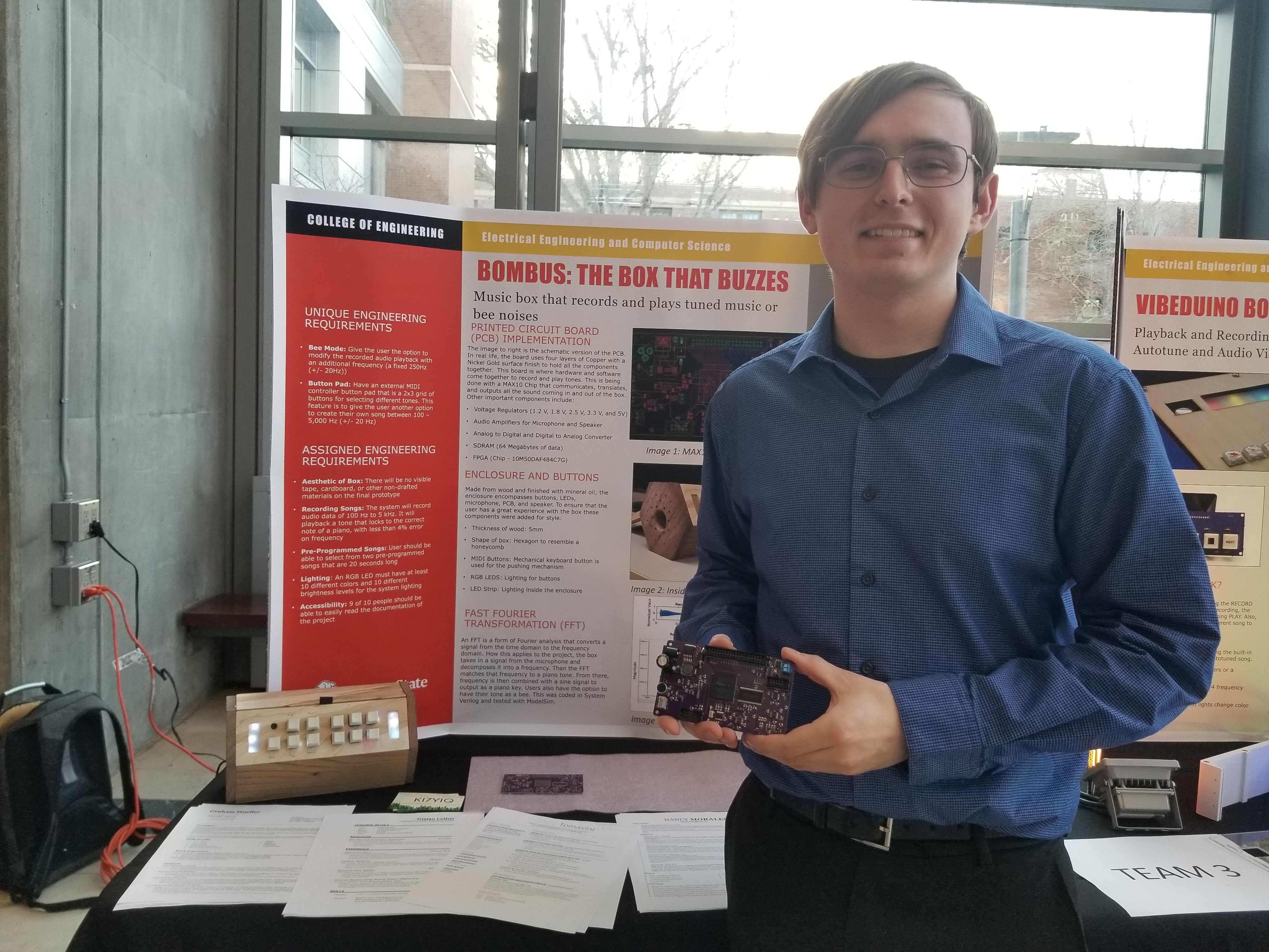
The project timeline must fit in an Oregon State University term (10 weeks) and by the time design, CAD, manufacturing, coding, etc. was done 9 weeks had passed. We had a working project thanks to development with the DE-10 Lite boards that were give to us in ECE 272: Digital Logic Design Lab (also featured the MAX 10 FPGA) and using the peripherals on the Max 10 Pollen Board that had header pins that could be connected to the GPIO of the DE-10. We presented our project with pride at the Junior Design Expo and acknowledged that we had probably learned more than most groups due to the scope of our project.
In the end, thanks the great effort from everyone in the Design Group, Matthew Shuman, Hi-Tek Electronics we made our Music Box for the Junior Design Expo. Here is the presentation video that we made to accompany the project to showcase how everyone contributed.
Here’s the GitHub link to the project repository (including EAGLE files).
Here’s the User Manual I wrote up so someone else could pick up this board and start using it with Quartus.
Here’s the Bill of Materials for the Max 10 Pollen Board.
| BOM Item # | Item Name | Quantity | Price/Unit | Total Cost |
|---|---|---|---|---|
| 1 | 0.1uF 0805 Capacitor | 1 | $0.01 | |
| 2 | 4pF 0805 Capacitor | 2 | $0.01 | |
| 3 | 0.01uF (10nF) 0805 Capacitor | 6 | $0.01 | |
| 4 | 1nF 0805 Capacitor | 1 | $0.01 | |
| 5 | 10uF 0805 Capacitor | 2 | $0.01 | |
| 6 | 1uF 0805 Capacitor | 9 | $0.01 | |
| 7 | 4.7uF 0805 Capacitor | 5 | $0.01 | |
| 8 | 0.47uF 0805 Capacitor | 1 | $0.01 | |
| 9 | 0.39uF 0805 Capacitor | 1 | $0.01 | |
| 10 | 1uF Tant Capacitor | 1 | $0.02 | |
| 11 | MBR360G DO201-15 | 1 | $0.50 | |
| 12 | 220ohm Ferrite Bead 0603 | 2 | $0.01 | |
| 13 | 30ohm Ferrite Bead 0603 | 3 | $0.01 | |
| 14 | INA332AIDGKR SOP65 | 1 | $1.61 | |
| 15 | LM4991MAX_NOPB | 1 | $1.35 | |
| 16 | LM2576HVS-12 | 1 | $6.57 | |
| 17 | IS42S16400J-7TLI | 1 | $1.83 | |
| 18 | CDCE937PWRG4 | 1 | $4.12 | |
| 19 | AD5320IDBVR | 1 | $6.25 | |
| 20 | ADS7868IDBVR | 1 | $1.55 | |
| 21 | MCP1726T-ADJE_SN | 4 | $0.68 | |
| 22 | REF3125AQDBZRQ1 | 1 | $2.81 | |
| 23 | 2x5 Shrouded Connector | 2 | $0.00 | |
| 24 | 2x20 Shrouded Connector | 1 | $0.00 | |
| 25 | 40-pin Male Header Pins | 1 | $0.00 | |
| 26 | SRR1260-101M 100uH Inductor | 1 | $1.25 | |
| 27 | 3mm LED | 1 | $0.05 | |
| 28 | Electret Microphone | 1 | $0.50 | |
| 29 | 24MHz CTS406 | 1 | $0.98 | |
| 30 | 2.2k 0805 Resistor | 3 | $0.01 | |
| 31 | 20k 0805 Resistor | 2 | $0.01 | |
| 32 | 4.7k 0805 Resistor | 7 | $0.01 | |
| 33 | 18.2 0805 Resistor | 3 | $0.01 | |
| 34 | 10k 0805 Resistor | 2 | $0.01 | |
| 35 | 1 0805 Resistor | 1 | $0.01 | |
| 36 | 1k 0805 Resistor | 1 | $0.01 | |
| 37 | 220 0805 Resistor | 1 | $0.01 | |
| 38 | 510k 0805 Resistor | 1 | $0.01 | |
| 39 | 100k 0805 Resistor | 1 | $0.01 | |
| 40 | 150k 0805 Resistor | 1 | $0.01 | |
| 41 | 510k 0805 Resistor | 1 | $0.01 | |
| 42 | 86k 0805 Resistor | 1 | $0.01 | |
| 43 | 12k 0805 Resistor | 1 | $0.01 | |
| 44 | 40k 0805 Resistor | 1 | $0.01 | |
| 45 | 20k 0805 Resistor | 1 | $0.01 | |
| 46 | 0.4 0805 Resistor | 1 | $0.01 | |
| 47 | 2.1mm DC Barrel Jack Connector | 1 | $0.40 | |
| 48 | 10k 10mm Potentiometer | 1 | $0.20 | |
| 49 | 10M50DAF484C7G FPGA | 1 | $150.80 | |
| 50 | E3.5-10 Electrolytic Capacitor 1000uF | 1 | $0.89 | |
| 51 | E5-6 Electrolytic Capacitor 100uF | 1 | $0.35 | |
| 52 | 220 Ohm Resistor | 21 | $0.05 | |
| 53 | Single 3mm RGB LED | 6 | $0.01 | |
| 54 | RGB LED Strip | 1 | $5.99 | |
| 55 | 8 Ohm 3W Speaker | 1 | $3.91 | |
| 56 | 9V AC-DC Power Jack | 1 | $13.90 | |
| $210.28 |